What H&T ‘s possession technology / Specialty fields & Areas of expertise.
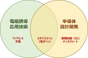
H&T ‘s possession technology

- Applications of Electromagnetic induction technology
<Electronic pen / wireless charging fields>
We specialize in the design and development of devices that use wireless charging technology, including electromagnetic induction electronic pens (stylus pens), and we also hold patents for electronic pens that feature unique pen pressure sensing.
- Technology of Analog & Mixed signal IC design
<Semiconductor field>
"Technology + Experience / Know-How" is the decisive factor for Analog ! H&T Technology has abundant experience and achievements in designing and developing high-frequency analog ICs for various applications such as communication, broadcasting, vehicle, and AV equipment.
- Design and development technology of Discrete semiconductor
<Semiconductor field>
We also develop discrete semiconductors such as diodes, small signal transistors, power transistors, and thyristors.

Technical introduction of "H&T stylus pen"
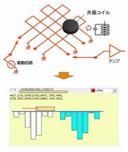
Operating principle of electronic pen
H&T ‘s stylus pen applies the principle of electromagnetic induction to detect the presence and pressure of the pen.
When the electronic pen is brought closer to the touch pen sensor, the value of the electromagnetic coupling between the coil of the orthogonal cell part in the sensor and the resonance coil of the electronic pen changes.
The change in the value of this electromagnetic coupling is captured as a signal, and the coordinate position is calculated from the output value of each cell in which the change in coupling is detected.
At that time, by detecting the phase, pen down and pen pressure are detected.
Unique electronic pen technology developed by H&T Technology
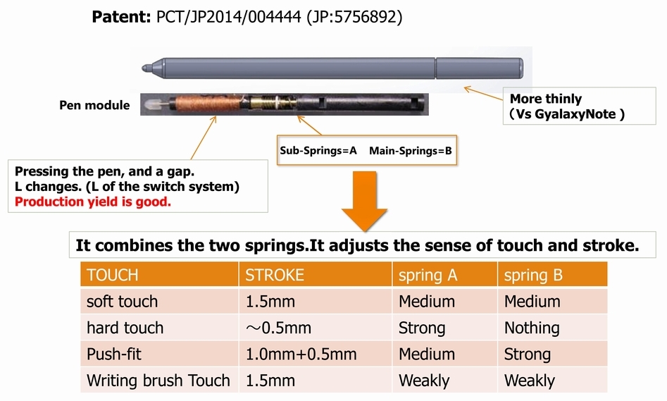
[Part 1] "Pressure detection technology" that realizes excellent drawing performance and natural writing comfortable.
◆Original pen pressure detection technology (patented)
H&T Technology has developed a unique pen pressure sensing technology (patented) by making full use of the semiconductor and electromagnetic induction technology cultivated to realize a simple and high-performance low-cost electronic pen.
H&T’s stylus pen can express the strength, color depth, touch feeling, etc. when drawing, the drawing performance is excellent, so you can experience the fun of pen writing & drawing.
In addition, it is battery-free and can be stored in a smartphone or tablet, making it convenient to carry!
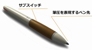
Electronic pen developed by H&T with a unique pen pressure detection mechanism
(Patented)
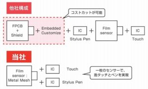
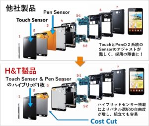
[Part 2] H&T's unique "hybrid touch pen sensor technology"
◆Hybrid sensor technology that enables low-cost products
H&T Technology has developed its own hybrid touch pen sensor, succeeded in reducing the number of parts and mounting costs to achieve the low cost!
Conventional electronic pens with electromagnetic induction have two types of sensors a finger touch sensor & a pen sensor, in which, it is difficulty of adjusting these sensors has been an obstacle to their adoption.
H&T Technology has achieved a finger touch sensor and a pen sensor with a single hybrid sensor. It becomes more fixable in panel selection, simplifies assembly, and enables low-cost products.
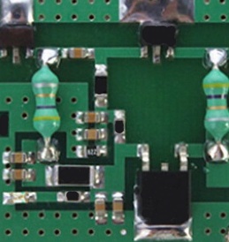
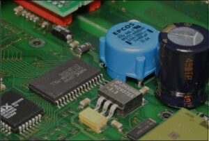
Main development achievements in the semiconductor field
H&T Technology has designed and developed numerous semiconductor integrated circuits (ICs) and discrete semiconductors.
Below is an example of our major development achievements.
◆ACMF (Active Common Mode Filter)
Development results
- ACMF IC for MIPI
- ACMF IC for HDMI
- ACMF IC for USB3.0
- ACMF IC for LAN 100/1000 Base
- ACMF IC for in-vehicle network CAN
Features of developed products
- Achieve common mode filter as IC in CMOS process
- High-frequency analog IC that eliminates common mode noise in a wide band with high efficiency
- Especially effective in high-definition transmission lines such as surveillance cameras, vehicle camera LVDS, smart TV cameras, etc.
LNA(ローノイズアンプ)
Development results
- LNA IC for terrestrial digital TV broadcasting
- LNA IC for BS/CS satellite broadcasting
Features of developed products
- Small size and low cost can be achived by CMOS process replacing GaAs and SiGe (silicon germanium).
- Low power consumption
OSCILLATOR
Development results
- Ultra-low noise crystal oscillation IC for Hi-Resolution audio
- IC for wideband clock generator
- Silicon oscillator IC that does not require an external oscillator
Features of developed products
- Application of our ultra-low noise circuit technology to oscillation Ics
- Optimal for applications requiring high-precision digital modulation technology, useful for development of high-resolution audio equipment
SWITCH (semiconductor switch)
Development results
- Ultra-low on-resistance load switch
ON resistance 1Ω ±15V power supply compatible - Single Pole/Single Throw (SPST) Analog Switches
Features of developed products
- Developed various semiconductor switches using low on-resistance technology
- Provides an ideal solution for test-equipment and measurement systems where” ultra-low on resistance”,” on-resistance flatness” and” low distortion” are important.
MEMSセンサー
Development results
- 3-axis accelerometer
- 9-axis motion sensor
- Digital pressure sensor
Features of developed products
- Simultaneously achieves miniaturization, power saving, and high noise immunity
(※)MEMS:Micro Electro Mechanical Systems
*If you would like to know more about our development achievements, please do not hesitate to contact us using the information below.